


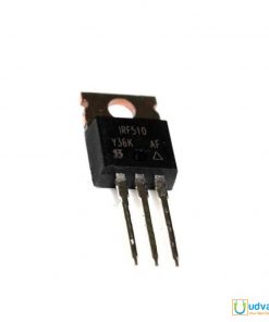
IRF650PBF IRF650 IRF 650 200V 28A 156W TO-220 N-Channel Power MOSFET 3 Pin IC Power Transistor Field Effect MOSFET IC Electronic Components
৳ 60.00
IRF650PBF IRF650 IRF 650 200V 28A 156W TO-220 N-Channel Power MOSFET 3 Pin IC Power Transistor Field Effect MOSFET IC
Out of stock
Description: IRF650 200V N-Channel MOSFET
IRF650PBF IRF650 IRF 650 200V 28A 156W TO-220 N-Channel Power MOSFET 3 Pin IC Power Transistor Field Effect MOSFET IC Electronic Components
These N-Channel enhancement mode power field effect transistors are produced using Fairchild’s proprietary, planar, DMOS technology. This advanced technology has been especially tailored to minimize on-state resistance, provide superior switching performance, and withstand high energy pulse in the avalanche and commutation mode. These devices are well suited for high efficiency switching DC/DC converters, switch mode power supplies, DC-AC converters for uninterrupted power supply and motor control.
Features:
28A, 200V, RDS(on) = 0.085 @VGS 10 V Low gate charge ( typical 95 nC) Low Crss ( typical 75 pF) Fast switching 100% avalanche tested Improved dv/dt capability
Parameter Drain-Source Voltage – Continuous (TC = 25°C) Drain Current – Continuous (TC = 100°C) Drain Current – Pulsed
Gate-Source Voltage Single Pulsed Avalanche Energy Avalanche Current Repetitive Avalanche Energy Peak Diode Recovery dv/dt Power Dissipation (TC = 25°C)
– Derate above 25°C Operating and Storage Temperature Range Maximum lead temperature for soldering purposes, 1/8″ from case for 5 seconds
* Drain current limited by maximum junction temperature.
Symbol RJC RCS RJA Parameter Thermal Resistance, Junction-to-Case Max. Thermal Resistance, Case-to-Sink Typ. Thermal Resistance, Junction-to-Ambient Max 2.51 -62.5 Units °C/W
BVDSS / TJ IDSS IGSSF IGSSR Drain-Source Breakdown Voltage Breakdown Voltage Temperature Coefficient Zero Gate Voltage Drain Current Gate-Body Leakage Current, Forward Gate-Body Leakage Current, Reverse VGS = 250 µA, Referenced to 25°C VDS 200 V, VGS 0 V VDS = 125°C VGS 30 V, VDS 0 V VGS -30 V, VDS V/°C µA nA
VGS(th) RDS(on) gFS Gate Threshold Voltage Static Drain-Source On-Resistance Forward Transconductance VDS = VGS, 250 µA VGS 14 A VDS 14 A
Ciss Coss Crss Input Capacitance Output Capacitance Reverse Transfer Capacitance VDS 25 V, VGS = 1.0 MHz pF
td(on) tr td(off) tf Qg Qgs Qgd Turn-On Delay Time Turn-On Rise Time Turn-Off Delay Time Turn-Off Fall Time Total Gate Charge Gate-Source Charge Gate-Drain Charge VDS 32 A, VGS 10 V
IS ISM VSD trr Qrr Maximum Continuous Drain-Source Diode Forward Current Maximum Pulsed Drain-Source Diode Forward Current VGS 28 A Drain-Source Diode Forward Voltage Reverse Recovery Time Reverse Recovery Charge VGS 32 A, dIF = 100 A/µs
Notes: 1. Repetitive Rating : Pulse width limited by maximum junction temperature = 1.15mH, IAS = 28A, VDD 25 , Starting 25°C 3. ISD 32A, di/dt 300A/µs, VDD BVDSS, Starting 25°C 4. Pulse Test : Pulse width 300µs, Duty cycle 2% 5. Essentially independent of operating temperature
Figure 3. On-Resistance Variation vs Drain Current and Gate Voltage
Figure 4. Body Diode Forward Voltage Variation with Source Current and Temperature
Specification:
- 28A, 200V, RDS(on) = 0.085Ω @VGS = 10 V
- Low gate charge ( typical 95 nC)
- Low Crss ( typical 75 pF)
- Fast switching
- 100% avalanche tested
- Improved dv-dt capability
- 5V gate allows for easy Arduino integration
- Shipped in static protective packaging and bubble mailers, NOT paper envelopes like other sellers
- GENUINE FAIRCHILD, Not knockoffs like most other sellers
- SUPER FAST SHIPPING: SHIPS FROM COLORADO, NOT CHINA
- U.S. ARMY SOCOM VETERAN OWNED BUSINESS
Package Include:
- 1 x IRF650 200V N-channel MOSFET
Only logged in customers who have purchased this product may leave a review.
Related products


Reviews
There are no reviews yet.