

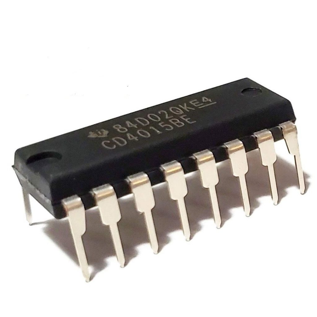
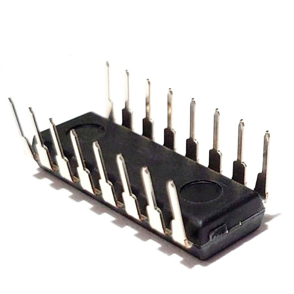
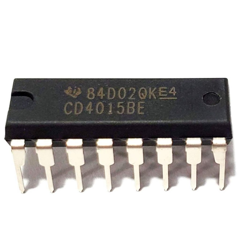
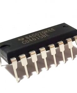


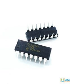
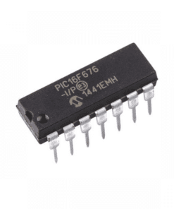
A Class CD4015BE CD4015 CD-4015 4015 DIP-16 Pin Dual In Package Dual 4 Stage Static Shift Register Serial In Parallel Out IC Breadboard Friendly IC
৳ 55.00
CD4015 4015 DIP-16 Pin Dual In Package Dual 4 Stage Static Shift Register Serial In Parallel Out IC Breadboard Friendly IC
Description: CD4015 IC CD 4015 DIP 16 Pin IC A Class
A Class CD4015BE CD4015 CD-4015 4015 DIP-16 Pin Dual In Package Dual 4 Stage Static Shift Register Serial In Parallel Out IC Breadboard Friendly IC
The CD4015 belongs to the CD4000 IC series. The IC contains two identical, 4-stage, serial input/parallel-output registers with independent “Data”, “Clock,” and “Reset” inputs. The logic level present at the input of each stage is transferred to the output of that stage at each positive-going clock transition. A logic high on the “Reset” input resets all four stages covered by that input. The IC has a wide range of operative conditions and voltages and interfaces directly with CMOS, NMOS, and TTL devices. CD4015 offers various features such as high noise immunity and low thermal dissipation.
What is Static Shift Register?
Static Shift registers are digital memory circuitry found in devices such as calculators, computers, and data processing systems. With a static shift register, data or bits are entered into the system in a serial or parallel manner. data entry is done from one direction, and as more data is added, it shifts positions until the data gets to the output end. The two ends are referred to as the left and right end. Movement of data can be from left to right, from right to left, or in both directions to make a bidirectional register.
CD4015 Key Features
- Wide supply voltage range: 3.0V to 18V
- High noise immunity: 0.45 VDD (typ.)
- Low power TTL: Fan out of 2 driving 74L compatibility: or 1 driving 74LS
- Medium speed operation: 8 MHz (typ.) clock rate
- Fully static design: @VDD − VSS = 10V
CD4015 Pinout
| Pin No | Pin Name | Description |
|---|---|---|
| 1 | CLK B | clock signal of shift register B |
| 2 | Q4B | output 4 of shift register B |
| 3 | Q3A | output 3 of shift register A |
| 4 | Q2A | output 2 of shift register A |
| 5 | Q1A | output 1 of shift register A |
| 6 | RA | reset value of shift register A |
| 7 | DA | data value of shift register A |
| 8 | VSS | source supply |
| 9 | CLK A | clock signal of shift register B |
| 10 | Q4A | output 4 of shift register A |
| 11 | Q3B | output 3 of shift register B |
| 12 | Q2B | output 2 of shift register B |
| 13 | Q1B | output 1 of shift register B |
| 14 | RB | reset value of shift register B |
| 15 | DB | data value of shift register B |
| 16 | VDD | Drain supply |
Application
- Serial-input/parallel-output data queuing
- Serial to parallel data conversion
- General-purpose register
Package Include:
- 1 x CD4015 IC CD 4015 DIP 16 Pin IC A Class
Only logged in customers who have purchased this product may leave a review.
Related products


Microcontroller, ICs & Base

Microcontroller, ICs & Base

Microcontroller, ICs & Base
PIC16F88 Microcontrollers IC 16F88 IC MCU DIP-28 28 Pin Leads Dual In Line Package Chip PIC16F88 IC

Microcontroller, ICs & Base
WIDE 40Pin Leads IC Socket IC Base 40 Pin PCB Mount IC Socket For 40 Pin Wide IC Base


Microcontroller, ICs & Base
PIC16F72 Microcontrollers IC 16F72 IC MCU DIP-28 28 Pin Leads Dual In Line Package Chip PIC16F72 IC

Microcontroller, ICs & Base


Microcontroller, ICs & Base


Microcontroller, ICs & Base

Microcontroller, ICs & Base
Microcontroller, ICs & Base

Microcontroller, ICs & Base

Microcontroller, ICs & Base

Microcontroller, ICs & Base


Microcontroller, ICs & Base

Microcontroller, ICs & Base


Microcontroller, ICs & Base


Microcontroller, ICs & Base


Microcontroller, ICs & Base


Microcontroller, ICs & Base

Microcontroller, ICs & Base


Microcontroller, ICs & Base

Microcontroller, ICs & Base


Microcontroller, ICs & Base


Microcontroller, ICs & Base
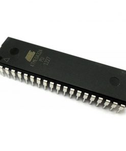
ATMEGA8A-PU ATMEGA8A Microcontroller ATMEGA8 IC 16MHz DIP 28 Pin Leads AVR Microcontroller IC

Microcontroller, ICs & Base

Microcontroller, ICs & Base

Microcontroller, ICs & Base

Microcontroller, ICs & Base

Reviews
There are no reviews yet.