

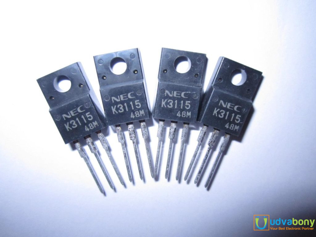
2SK3115 2SK-3115 K3115 3115 MOSFET 450V 6A TO-220 Field Effect Transistor Silicon N-Channel Power MOSFET Transistor
৳ 40.00
2SK3115 2SK-3115 K3115 3115 MOSFET 450V 6A TO-220 Field Effect Transistor Silicon N-Channel Power MOSFET Transistor
Description: 2SK3115 N-Channel DMOS FET
2SK3115 2SK-3115 K3115 3115 MOSFET 450V 6A TO-220 Field Effect Transistor Silicon N-Channel Power MOSFET Transistor
The 2SK3115 is N-Channel DMOS FET device that features a low gate charge and excellent switching Characteristics, and designed for high voltage applications such as switching power supply, AC adapter
Features:
Low gate charge 26 nC TYP. (VDD 450 V, VGS = 6.0 A) Gate voltage rating ±30 V Low on-state resistance RDS(on) = 1.2 MAX. (VGS = 3.0 A) Avalanche capability ratings . Drain to Source Voltage (VGS 0 V) Gate to Source Voltage (VDS 0 V) Drain Current (DC) (TC = 25°C) Drain Current (pulse)
Total Power Dissipation (TA = 25°C) Total Power Dissipation (TC = 25°C) Channel Temperature Storage Temperature Single Avalanche Current Single Avalanche Energy The information in this document is subject to change without notice. Before using this document, please confirm that this is the latest version.
Not all devices/types available in every country. Please check with local NEC representative for availability and additional information.
Document No. D13338EJ2V0DS00 (2nd edition) Date Published January NS CP (K) Printed in Japan
Characteristics Zero Gate Voltage Drain Current Gate Leakage Current Gate Cut-off Voltage Forward Transfer Admittance Drain to Source On-state Resistance Input Capacitance Output Capacitance Reverse Transfer Capacitance Turn-on Delay Time Rise Time Turn-off Delay Time Fall Time Total Gate Charge Gate to Source Charge Gate to Drain Charge Body Diode Forward Voltage Reverse Recovery Time Reverse Recovery Charge Symbol IDSS IGSS VGS(off) | yfs | RDS(on) Ciss Coss Crss td(on) tr td(off) tf QG QGS QGD VF(S-D) trr Qrr VDD 450 V VGS 6.0 A, VGS 6.0 A, VGS 0 V di/dt = 50 A/µs Test Conditions VDS 600 V, VGS 0 V VGS ±30 V, VDS 0 V VDS 1 mA VDS 3.0 A VGS 3.0 A VDS 10 V VGS MHz VDD 3.0 A VGS(on) , RL MIN. TYP. MAX. ±100 3.5 Unit
Package Include:
- 1 x 2SK3115 N-Channel DMOS FET
Only logged in customers who have purchased this product may leave a review.
Related products


MOSFETs & IGBTs
2SK1794 2SK-1794 K1794 1794 MOSFET 900V 6A 100W TO-3P Field Effect Transistor MOSFET


MOSFETs & IGBTs
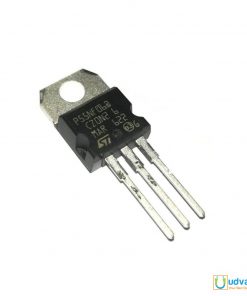
P55NF06 IC STP55NF06 55NF06 55N06 MOSFET 55A 60V 95W N-Channel TO-220 3 Pin Leads MOSFET IC


MOSFETs & IGBTs
2SK2508 2SK-2508 K2508 2508 MOSFET 250V 13A TO-220 Switching N-Channel Power MOSFET Transistor


Reviews
There are no reviews yet.